2015 News Release
Hitachi, Ltd.
Hitachi Metals, Ltd.
Hitachi Developed Ceramic Package Substrate to Enhance Data Processing Capability Ten Times Greater in Information Technology Equipment
Achieving high reliability and low cost package substrate compared with silicon interposer package
Hitachi, Ltd. (TSE: 6501) and Hitachi Metals, Ltd. (TSE: 5486) have developed the LTCC (Low Temperature Co-fired Ceramics)1package substrate with 2μm2 line and space re-distribution layer (RDL). Compared with current package substrate3 LTCC package substrate has achieved more than ten times of data processing capability by connecting LSI dies with memory dies by more than 1,000 fine lines. Furthermore, the capability of high reliability and low cost of this package substrate compared with the organic package substrate with silicon interposer4 are also shown.
In recent years, much attention has been placed on the Internet of Things (IoT). As the IoT spreads, it is inevitably to perform real-time processing of the massive volume of data from internet connected devices such as sensors, cameras, home appliances, or smart devices in automobiles. To enhance the data processing capability of these devices, increase of data transfer rate and number of signals are required. Conventionally, many advanced technologies have been proposed to the development of improving data processing capability. One of these technologies is the silicon interposer stacked with organic package substrate on which several thousands of μm width wires are fabricated. However, silicon interposer fabrication includes a costly process of forming through silicon via and thinning wafer. The thinned silicon interposer will be stacked on an organic substrate. Both cost and reliability are the obstacles for adapting silicon interposer.
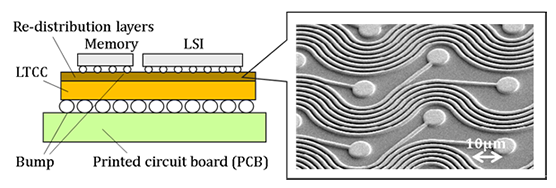
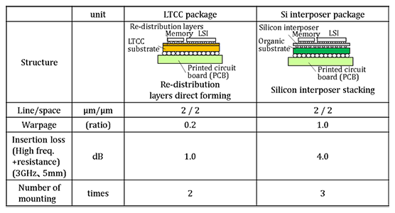
Therefore, Hitachi and Hitachi Metals focused on the technology of LTCC to develop the LTCC package substrate with fine line layers (Fig.1). This newly developed LTCC package substrate is capable of forming thin film layers directly on a LTCC substrate. This has not only eliminated the use of silicon interposer, but also removed one process step from assembly flow, which achieves a low cost manufacturing. Also, due to the coefficient of thermal expansion5 of the LTCC substrate is close to LSI dies and memory dies compared with the organic substrate, the warpage of substrate by thermal expansion during soldering process is smaller, which enhances its reliability. Furthermore, the LTCC substrate is capable of forming thicker lines compared with the silicon substrate, which is capable of minimizing the insertion loss6 (Table 1).
The features of the developed LTCC package substrate are listed as below:
1.The LTCC substrate is capable of formulating fine lines.
Photolithography7 technology is used for the formation of fine lines. Any warpage and unevenness on substrate could cause defocusing to prevent fine lines formation at stepper exposure process. Also, the characteristic of ceramic material’s sintering shrinkage affects the position error between the lines on fine line layer formed by photolithography and on the ceramic substrate. This will be more serious when lines become fine. As to solve this difficulty, Hitachi Metals has developed extremely precise polishing technology that can reduce warpage and unevenness of LTCC substrate, and developed sintering technology that can reduce shrinkage in x/y direction during sintering by constraining the x/y direction of the LTCC substrate. In consequence, these technologies achieves the formation of 2μm line and space on the LTCC package substrate.
2.Fine line is achieved by the technology of electrical characteristics analysis and LSI stress analysis.
As the cross-section area becomes smaller with the μm sized wiring lines, its current density will increase that causes the increase of the loss from wiring resistance8. Therefore, fine wiring lines should be designed by considering insertion loss by wiring resistance in addition to the loss of high frequency.
Hitachi has developed a technology of electrical characteristics analysis that can accurately analyze both the loss of wiring resistance and high frequency. This technology is capable of optimizing the structure of fine lines to design fine lines with lower loss (Fig.1).
Furthermore, the bump9 that bonds LSI dies and LTCC package substrate is exceptionally fine as 20μm for increasing the number of line. We have also developed the technology of LSI package stress analysis to analyze the stress on this micro bump. This technology is capable of optimizing the structure of micro bump to bond LSI dies and memory dies to LTCC package substrate with high reliability.
We are committing to promote further low cost in LTCC package substrate in order to make contributions of building social infrastructure with safety and comfort.
The achievement of this research will be presented on 14th December at the 2015 IEEE Design of Advanced Packaging & Systems (EDAPS) Symposium, which will be held in Seoul, South Korea.
- *1
A substrate is made from a material that is to add alumina (Aluminium oxide that is one of ceramic, which is commonly used in various industries.) to glass to enable it to be fired at low temperature. It is used as the substrate of parts in such as cell phones due to its feature of low firing temperature that enables the use of high-conductivity wiring materials (Silver and Copper). - *2
Micrometer (μm) is a unit of measure, 1μm is equal to 0.001 mm. - *3
LSI and memory are separately mounting to different packaging substrate. - *4
The silicon chip only forms wires, which connects between multilayer LSIs while interconnects between LSI and organic package. - *5
The ratio of thermal expansion of object’s volume from temperature. - *6
Part of energy from input signal are converted to heat from a characteristic of dielectric and wiring resistance. - *7
Fine pattern fabrication technology using photo technology. - *8
The difficulty of current flow. - *9
Metal bump on the electrodes of LSI and package substrate, to be used for connecting wires on substrate.
-
 Fig. 1 Structure and fine line of developed LTCC package substrate
 -
 Table 1 A comparison of silicon interposer package and developed LTCC package
For inquiries from customers:
Magnetic Materials Company, Hitachi Metals, Ltd.
Soft Magnetic Materials and Applications (soft ferrite)