2010 The former Hitachi Cable News Release
Information (including product prices, product specifications, details of services, launch dates, inquiry information, and URLs) contained in this news release is current as of the date of the press release but is subject to change without notice. Please note that details may differ from those effective on the search date.
Hitachi Cable develops world's first lead-free piezoelectric film
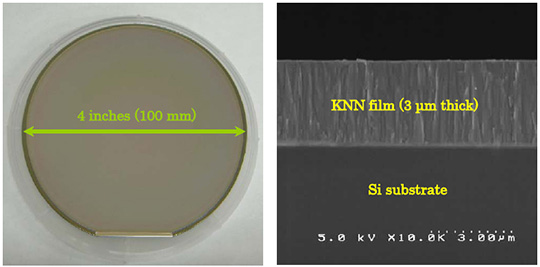
Hitachi Cable, Ltd. announced the successful development of a lead-free piezoelectric film with a piezoelectric constant*1 exceeding 100 pm/V for the first time anywhere in the world,*2 as well as success in producing a film of this material measuring 4 inches in diameter via sputtering.
Piezoelectric films are thin films composed of piezoelectric materials-materials that generate a voltage when subjected to mechanical strain. Conversely, the application of a voltage to these materials will generate mechanical strain. One of the most commonly used materials for piezoelectric films is lead (Pb) zirconate titanate (PZT). This material is used in camera shake sensors in digital cameras, vehicle roll-over sensors, and print heads in piezoelectric inkjet printers.*3
Growing numbers of devices incorporate devices based on piezoelectric films, and future applications are likely to include MEMS mirrors for projectors*4,*5 and small vibration-powered generators.
While growing environmental awareness has forced the use of lead-free materials, creating piezoelectric films based on lead-free materials capable of achieving a piezoelectric constant adequate for practical use has posed a significant challenge. The properties of the materials actually used require significant improvement.
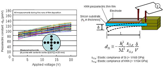
We have succeeded in developing a lead-free piezoelectric film with a piezoelectric constant exceeding 100 pm/V, and have produced a film of this material measuring 4 inches in diameter via sputtering.
Our lead-free film uses potassium sodium niobate (KNN) as its piezoelectric material. Among lead-free piezoelectric materials, KNN in bulk ceramic form*6 is known to have a high Curie temperature*7 and ideal piezoelectric properties. However, few reports have discussed the formation of KNN into films, and forming very fine KNN films with c-axis orientation*8 adequate to produce the desirable piezoelectric properties is difficult.
To address these issues, we developed technologies for forming KNN into a very fine film with high c-axis orientation by optimizing film deposition conditions. Additionally, through heat treatment applied after film deposition, we reduced residual stress, which can significantly affect orientation and piezoelectric properties. Ultimately, we achieved a piezoelectric constant exceeding 100 pm/V, a figure comparable to existing PZT piezoelectric films, for the world's first lead-free piezoelectric film suitable for practical applications.
Sputtering is the film deposition method used to make this film. This process creates a large film with high reproducibility, making it ideal for mass production. We have used our sputtering system to form films of up to 4 inches in diameter.
We plan to pursue research and development to establish technologies for the mass-production of 4-inch films and to improve the piezoelectric properties of these films still further.
We will give a presentation on this development in an upcoming lecture (lecture No.16p-NJ-10, 16p-NJ-14, and 16p-NJ-15) at the 71st Fall Meeting, 2010, of the Japan Society of Applied Physics, to be held at Nagasaki University's Bunkyo Campus from September 14 to 17, 2010.
| *1 | The piezoelectric constant indicates to what extent an element is strained when a voltage is applied. Here, it refers to d31. |
| *2 | As of March 19, 2010, this is the world's only lead-free piezoelectric film to achieve a piezoelectric constant exceeding 100 pm/V (pm = 10-12m). This figure was verified in our testing. |
| *3 | A piezoelectric inkjet printer uses piezoelectric elements in its ink nozzles. |
| *4 | MEMS stands for micro-electro-mechanical system. A MEMS is a very small electro-mechanical component that combines a mechanical component with an electronic circuit. |
| *5 | A MEMS mirror is a microscopic component with a mirror whose reflective angle changes when subjected to electric current. |
| *6 | Bulk ceramics are sintered compacted materials bonded by high heat treatment. Bulk ceramics are brittle and difficult to microfabricate. |
| *7 | The Curie temperature is the temperature at which a ferroelectric material becomes paraelectric or a ferromagnetic material becomes paramagnetic. Piezoelectric properties are lost above the Curie temperature. |
| *8 | The c-axis is one of the crystal axes used to depict a crystal in three dimensions. |
Appearance and cross section of a potassium-sodium-niobate piezoelectric film
Piezoelectric properties of a potassium-sodium-niobate piezoelectric film